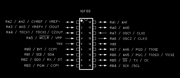
16F88 Physical Input and Output
The 16F88 has 16 I/O pins
These pins are accessed via port A and B
To identify which bit within which port is responsible for driving a
particular PIC pin, look at the pin diagram below (this diagram is only
good for the 16F88, refer to other pin diagrams for other PICs). Locate
the pin you are interested in and read off the label.
The label will be of the form Rxj
where x will be A for PORTA, B for PORTB etc.,
and j will be the bit number within the port (in the range
0 to 7)
On the 16F88 port A bit 0 connects to the pin labelled
RA0 which is pin 17, port A bit 3 connects
to the pin labelled RA3 which is pin 2
NOTE: most of the I/O pins on the 16F88 have multiple
functions and multiple labels to indicate these functions. When using a
pin it must be configured to perform the required function. This is done
internally by the program when it starts running. The program writes to
special function registers which are responsible for configuring the
pins.
| LABEL |
PIN |
|
PIN DIAGRAM |
| |
| RA0 |
17 |
|
 |
| RA1 | 18 |
| RA2 | 1 |
| RA3 | 2 |
| RA4 | 3 |
| RA5 | 4 |
| RA6 | 15 |
| RA7 | 16 |
| | |
| RB0 | 6 |
| RB1 | 7 |
| RB2 | 8 |
| RB3 | 9 |
| RB4 | 10 |
| RB5 | 11 |
| RB6 | 12 |
| RB7 | 13 |
sample projects (ciruits, sample code and chip programming)
XCSB compiler
Writing to a specific pin
To write to pin 1 of a 16F88 lookup the label on pin 1
in the pin diagram. The label is RA2. This translates to PORTA
bit 2.
| BIT NUMBER |
7 |
6 |
5 |
4 |
3 |
2 |
1 |
0 |
| PORTA |
x |
x |
x |
x |
x |
x |
x |
x |
| TRISA |
x |
x |
x |
x |
x |
x |
x |
x |
| PIN LABEL |
RA7 |
RA6 |
RA5 |
RA4 |
RA3 |
RA2 |
RA1 |
RA0 |
| PIN NUMBER |
16 |
15 |
4 |
3 |
2 |
1 |
18 |
17 |
Clear the corresponding bit in the PORTA data direction
register (called TRISA) to 0, that is clear TRISA bit
2 to 0. This configures pin 1 as an output.
| BIT NUMBER |
7 |
6 |
5 |
4 |
3 |
2 |
1 |
0 |
| PORTA |
x |
x |
x |
x |
x |
x |
x |
x |
| TRISA |
x |
x |
x |
x |
x |
0 |
x |
x |
| PIN LABEL |
RA7 |
RA6 |
RA5 |
RA4 |
RA3 |
RA2 |
RA1 |
RA0 |
| PIN NUMBER |
16 |
15 |
4 |
3 |
2 |
1 |
18 |
17 |
Then write the required value (0
or 1) to PORTA bit 2
| BIT NUMBER |
7 |
6 |
5 |
4 |
3 |
2 |
1 |
0 |
| PORTA |
x |
x |
x |
x |
x |
0 or 1 |
x |
x |
| TRISA |
x |
x |
x |
x |
x |
0 |
x |
x |
| PIN LABEL |
RA7 |
RA6 |
RA5 |
RA4 |
RA3 |
RA2 |
RA1 |
RA0 |
| PIN NUMBER |
16 |
15 |
4 |
3 |
2 |
1 |
18 |
17 |
This can be done in XCSB as:
// configure pin 1 as output by writing 0 to TRISA bit 2
TRISA = TRISA & ~0x04

// set pin 1 low (to 0) by writing 0 to PORTA bit 2
PORTA = PORTA & ~0x04

// set pin 1 high (to 1) by writing 1 to PORTA bit 2
PORTA = PORTA | 0x04
The 0x04 value is a hex mask (the equivalent of binary 00000100
see binary to hex).
A simpler way to access a bit within
a byte is to use a constant expression of the form
(1 << n)
where n is the bit number and
<< is the left shift operator
To access multiple bits within a byte, combine them with the bit wise OR operator
e.g.
(1 << n) | (1 << m) | (1 << j)
where n, m and j are the bit numbers
To set pins 1 and 17 to 1 use
TRISA = TRISA & ~((1 << 2) | (1 << 0))
PORTA = PORTA | ((1 << 2) | (1 << 0))
More about bit manipulation and binary
Reading from a specific pin
To read from pin 1 of a 16F88 lookup the label on pin 1
in the pin diagram. The label is RA2. This translates to PORTA
bit 2.
| BIT NUMBER |
7 |
6 |
5 |
4 |
3 |
2 |
1 |
0 |
| PORTA |
x |
x |
x |
x |
x |
x |
x |
x |
| TRISA |
x |
x |
x |
x |
x |
x |
x |
x |
| PIN LABEL |
RA7 |
RA6 |
RA5 |
RA4 |
RA3 |
RA2 |
RA1 |
RA0 |
| PIN NUMBER |
16 |
15 |
4 |
3 |
2 |
1 |
18 |
17 |
Set the corresponding bit in the PORTA data direction
register (called TRISA) to 1, that is set TRISA bit
2 to 1. This configures pin 1 as an input.
| BIT NUMBER |
7 |
6 |
5 |
4 |
3 |
2 |
1 |
0 |
| PORTA |
x |
x |
x |
x |
x |
x |
x |
x |
| TRISA |
x |
x |
x |
x |
x |
1 |
x |
x |
| PIN LABEL |
RA7 |
RA6 |
RA5 |
RA4 |
RA3 |
RA2 |
RA1 |
RA0 |
| PIN NUMBER |
16 |
15 |
4 |
3 |
2 |
1 |
18 |
17 |
Then read from PORTA and mask out bit 2
This can be done in XCSB as:
// configure pin 1 as input by writing 1 to TRISA bit 2
TRISA = TRISA | 0x04

// read 0 or 1 into the variable called result
result = (PORTA & 0x04) != 0

// NOTE: the expression (PORTA & 0x04) return 0x00 or 0x04
// the expression X != 0 return 0 if X is 0x00 or 1 if X is 0x04
The 0x04 value is a hex mask (the equivalent of binary 00000100
see binary to hex).
A simpler way to access a bit within
a byte is to use a constant expression of the form
(1 << n)
where n is the bit number and
<< is the left shift operator
The above example could then be re-written as:
// configure pin 1 as input by writing 1 to TRISA bit 2
TRISA = TRISA | (1 << 2)

// read 0 or 1 into the variable called result
result = (PORTA & (1 << 2)) != 0

// NOTE: the expression (PORTA & (1 << 2)) return 0x00 or 0x04
// the expression X != 0 return 0 if X is 0x00 or 1 if X is 0x04
More about bit manipulation and binary